X射线光刻
Search documents
SemiAnalysis--X射线光刻能否颠覆ASML+TSMC芯片制造格局?
傅里叶的猫· 2025-10-30 12:33
Core Viewpoint - The article discusses the potential disruption in the semiconductor industry brought by Substrate, a startup aiming to innovate chip manufacturing through its new X-ray lithography (XRL) technology, which promises significant cost reductions and performance improvements compared to existing methods [5][10][30]. Group 1: Industry Context - The semiconductor manufacturing industry has been dominated by inertia, with leading companies hesitant to deviate from established technologies despite rising costs and slowing scaling speeds [5][7]. - Current lithography tools, such as EUV, are highly profitable, making companies reluctant to abandon existing systems, which creates opportunities for innovative newcomers like Substrate [7][10]. Group 2: Substrate's Technology - Substrate aims to provide technological support for next-generation wafer fabs, focusing on significantly lowering the production costs of advanced logic wafers through its proprietary XRL tools [8][10]. - The XRL technology claims to overcome historical challenges associated with X-ray lithography, such as optical system and light source issues, and has demonstrated impressive performance metrics, including a resolution comparable to High-NA EUV [10][12]. Group 3: Performance Metrics - Substrate's XRL tool reportedly achieves single-exposure capabilities for 2nm and 1nm nodes, with a patterning accuracy of 1.6nm and a critical dimension uniformity (CDU) of 0.25nm [10][12]. - The company asserts that its technology can reduce production costs by 50% compared to current methods, although this claim requires further validation [10][13]. Group 4: Market Implications - If successful, Substrate's XRL technology could reshape the lithography landscape, providing a cost-effective alternative to existing high-cost tools, thus enhancing design flexibility and potentially increasing transistor density [16][18]. - The global lithography equipment market is projected to reach approximately $50 billion by 2030, and Substrate's technology could capture significant market share if it achieves mass production [18][30]. Group 5: Strategic Goals - Substrate's long-term vision includes establishing its own wafer fabrication facility, integrating XRL technology into a complete end-to-end chip manufacturing process [14][24]. - The company aims to contribute to the localization of chip manufacturing in the U.S., addressing concerns over reliance on foreign production, particularly from Taiwan [23][24]. Group 6: Challenges Ahead - Despite the promising technology, Substrate faces significant hurdles, including the need for larger exposure field sizes, equipment stability, and full-process validation to ensure compatibility across multiple layers [28][29]. - The transition from laboratory technology to commercial production is complex and may take several years, with industry experts noting that achieving mass production could take until around 2030 [29][30].


这个高中生,要挑战台积电
半导体芯闻· 2025-10-29 10:40
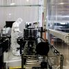
Core Viewpoint - The article discusses the emergence of Substrate, a startup founded by James Proud, which aims to revolutionize semiconductor manufacturing by developing a new, cost-effective lithography technology that could challenge the dominance of ASML and TSMC in the industry [1][4][19]. Group 1: Company Overview - Substrate has raised over $100 million from investors, including notable figures like Peter Thiel, and is valued at over $1 billion [4]. - The company plans to establish a manufacturing facility in the U.S. to reduce reliance on overseas suppliers, aligning with national security priorities [4][19]. - Substrate's technology involves using particle accelerators to create a new type of lithography tool, which could potentially lower manufacturing costs by half [1][3]. Group 2: Technology and Innovation - The startup aims to combine proprietary particle accelerators with custom lithography machines to achieve high-resolution microchip layers comparable to those produced by leading semiconductor manufacturers [1][13]. - Substrate claims its machines can print features at 12 nanometers, matching the capabilities of ASML's latest high-NA EUV machines [13][15]. - The company has demonstrated its system at U.S. national laboratories, achieving complex patterns on wafers [14]. Group 3: Challenges and Industry Reception - Despite significant funding and ambitious plans, Substrate faces skepticism from government scientists and the semiconductor industry regarding its ability to replicate the complex supply chain within three years [4][8]. - Concerns have been raised about the reliability of using a single particle accelerator as a light source for multiple tools, which could lead to factory downtime if it fails [8]. - The company has encountered challenges in securing government funding, with initial requests for over $1 billion from the CHIPS Act being rejected [8]. Group 4: Future Plans and Goals - Substrate aims to establish a vertically integrated foundry in the U.S. for custom semiconductor production, requiring significant capital investment potentially in the range of billions of dollars [19][20]. - The company is in discussions with Texas A&M University to build a particle accelerator and factory, with an estimated investment of around $10 billion [20]. - Proud emphasizes the need for innovative solutions in semiconductor manufacturing, stating that creating a better alternative is essential for the industry's future [21].

一个辍学生,同时挑战ASML和台积电
3 6 Ke· 2025-10-29 02:45
Core Insights - Substrate, a startup founded by James Proud, aims to revolutionize semiconductor manufacturing by developing a cost-effective alternative to ASML's advanced lithography machines, potentially reducing manufacturing costs by half [1][4][15] - The company has secured over $100 million in funding from notable investors, including Peter Thiel's Founders Fund, and is valued at over $1 billion [4][17] - Substrate's technology involves using a particle accelerator as a light source for X-ray lithography, which the company claims can achieve resolutions comparable to the latest ASML machines [12][13][15] Company Overview - Substrate was founded in January 2022 by James Proud and his brother Oliver, who have backgrounds in technology and entrepreneurship [6][7] - The company is based in San Francisco and has grown its team to 50, including engineers from major tech firms like TSMC, IBM, and Google [7] - Substrate's goal is to establish a manufacturing facility in the U.S. to reduce reliance on overseas suppliers, aligning with national security priorities [4][16] Technology and Innovation - Substrate's approach combines proprietary particle accelerator technology with customized lithography tools, aiming to commercialize a previously uncommercialized process [6][12] - The company claims to have achieved a resolution of 12 nanometers, suitable for producing chips at the cutting-edge 2-nanometer technology node [13][15] - Substrate emphasizes that it does not rely on externally produced lithography tools or intellectual property, claiming a differentiated technology [15] Market Position and Challenges - Despite significant funding and technological advancements, Substrate faces skepticism from industry experts regarding its ability to replicate the complex semiconductor supply chain within its projected timeline [4][8] - The company has encountered challenges in securing government funding and support, particularly from the Biden administration, which has raised concerns about its proposed funding requests [8][10] - Substrate's long-term vision includes becoming a major player in semiconductor manufacturing, potentially rivaling TSMC and ASML [16][17]

一个辍学生,同时挑战ASML和台积电
半导体行业观察· 2025-10-29 02:14
Core Viewpoint - The article discusses the emergence of Substrate, a startup founded by James Proud, which aims to revolutionize semiconductor manufacturing by developing a new technology that could significantly reduce production costs and challenge established players like ASML and TSMC [2][4][15]. Group 1: Company Overview - Substrate has raised over $100 million from investors, including Peter Thiel's Founders Fund, and is valued at over $1 billion [4]. - The company plans to establish a manufacturing facility in the U.S. to reduce reliance on overseas suppliers, aligning with national security priorities [4][17]. - Substrate's technology involves using a particle accelerator as a light source for a new type of lithography, which could potentially match the resolution of ASML's advanced machines [12][15]. Group 2: Technology and Innovation - The startup aims to combine proprietary particle accelerator technology with custom lithography tools to achieve commercial viability [12][15]. - Substrate claims its machines can print features at 12 nanometers, comparable to the latest high-NA EUV machines from ASML [13][15]. - The company has demonstrated its system at national laboratories, creating complex patterns on wafers [13]. Group 3: Challenges and Market Position - Substrate faces skepticism from industry experts regarding its ability to replicate the complex semiconductor supply chain within three years [4][8]. - The company has encountered challenges in securing funding from government initiatives, with initial requests for over $1 billion being denied [8]. - Despite the challenges, Substrate's founders believe that their approach could provide a viable alternative in the semiconductor market, especially as the U.S. seeks to bolster its domestic manufacturing capabilities [18].