半导体芯闻
Search documents
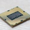
为了HBM 4,SK海力士准备扫货
半导体芯闻· 2025-10-24 10:34
Core Insights - SK Hynix is preparing to invest in testing equipment for the mass production of HBM4, with plans to establish a supply chain by the end of this year and begin equipment installation in Q1 of next year [1] - HBM4, the next generation of high bandwidth memory, will feature double the number of I/O terminals compared to its predecessor, significantly enhancing bandwidth [1] - The company aims to build new aging testing facilities to expand HBM4 mass production, with initial orders for equipment expected to be completed by October or November [1] Group 1 - SK Hynix plans to launch aging testing equipment for HBM4 in Q1 of next year, following successful quality tests by partners [1] - The aging testing equipment is designed to expose semiconductors to high temperatures and voltages to identify defects, and previous equipment was insufficient for HBM4 production [1] - A significant order of approximately 150 to 200 aging testing machines is anticipated as SK Hynix seeks to improve yield and productivity in the competitive HBM4 market [2] Group 2 - Major post-processing equipment companies in South Korea, such as DI, YC, and UniTest, are conducting quality tests to secure a place in SK Hynix's HBM4 aging testing equipment supply chain [2] - DI has recently completed quality testing with SK Hynix and is expected to be among the first to respond to initial orders, while UniTest and YC aim to complete supply by the end of the year [2] - The semiconductor industry anticipates that SK Hynix will actively invest in the expansion of the M15X wafer fab next year, indicating a strategic diversification of the aging testing equipment supply chain [2]


刚刚,沐曦过会
半导体芯闻· 2025-10-24 10:34
Core Viewpoint - The article highlights the successful approval of domestic GPU company Muxi by the China Securities Regulatory Commission, marking a significant milestone for the domestic GPU market and its potential to challenge foreign dominance in the sector [1][3]. Company Overview - Muxi focuses on the research, design, and sales of high-performance GPU chips and computing platforms, primarily for artificial intelligence training, inference, general computing, and graphics rendering [3][4]. - The company has developed a unique GPU product system and an open software ecosystem, contributing to the autonomous and controllable development of China's intelligent computing infrastructure [4][5]. Market Position and Strategy - Muxi aims to contribute to national technological advancement and digital economy growth, positioning itself as a leading player in the high-performance GPU market [4][5]. - The company has been actively breaking the monopoly of foreign manufacturers in the GPU market, leveraging its innovative products and technologies to increase market share [4][5]. Product Development - Muxi's product line includes the Xisi N series for inference, the Xiyun C series for integrated training and general computing, and the upcoming Xicai G series for graphics rendering [6][7]. - The GPUs are based on self-developed GPU IP and a unified architecture, showcasing strong competitiveness in performance, stability, and ecosystem compatibility [6][7]. Ecosystem and Collaboration - Muxi has established extensive collaborations across the ecosystem, optimizing performance for distributed inference in large models and supporting the commercialization of domestic computing power [7][8]. - The company has deployed its products in over ten intelligent computing clusters across various regions, enhancing capabilities in sectors such as education, finance, transportation, energy, healthcare, and entertainment [7][8]. Recent Innovations - At the 2025 World Artificial Intelligence Conference, Muxi launched its flagship GPU, the Xiyun C600, which signifies a historic breakthrough for domestic high-performance GPUs [7][8]. - The Xiyun C600 features a fully domestic supply chain and advanced capabilities, including large-capacity storage and multi-precision mixed computing, aimed at meeting the demands of next-generation generative AI [8].

雷军:最近内存涨得太多了
半导体芯闻· 2025-10-24 10:34
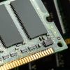
Core Viewpoint - The rising prices of memory chips are impacting the pricing of new smartphone products, as highlighted by Xiaomi's recent product launch and statements from its executives [1][2]. Group 1: Product Launch and Pricing - Xiaomi's REDMI K90 series was launched with starting prices of 2599 yuan for K90 and 3999 yuan for K90 Pro Max, which some consumers perceive as too high [1]. - Xiaomi's founder and CEO Lei Jun acknowledged the significant increase in memory costs, urging consumers to understand the company's pricing decisions [1]. Group 2: Memory Chip Price Surge - Major memory chip manufacturers like Samsung and SK Hynix are expected to raise prices of DRAM and NAND products by up to 30% due to increased demand [2]. - The demand for storage chips has surged due to the rapid growth of AI technologies, with AI server storage capacity needs being 8-10 times greater than traditional servers [1][2]. Group 3: Market Trends and Predictions - The AI boom is driving a "super cycle" in the storage chip industry, with Morgan Stanley predicting significant growth [2]. - TrendForce forecasts a quarterly increase of 8% to 13% in general DRAM prices and a 5% to 10% rise in NAND Flash prices in the fourth quarter [2]. - The price increase trend for AI server storage products is expected to continue until 2026, benefiting domestic storage companies through price recovery and domestic substitution [2].
存储芯片大厂要涨价,要求签长约
半导体芯闻· 2025-10-23 09:58
Core Insights - The demand for memory semiconductors, particularly high bandwidth memory (HBM) and general DRAM, is surging due to the explosive growth of data generated by AI entities like OpenAI and Gemini [1][2] - Major electronic and IT companies in the US and China are negotiating long-term DRAM supply contracts with Samsung Electronics and SK Hynix to secure inventory amid concerns of DRAM shortages [1][2] - The combined market share of Samsung Electronics and SK Hynix in the global general DRAM market exceeds 70%, and both companies are shifting their investment focus towards HBM, leading to a decline in general DRAM production capacity [2][3] Demand and Supply Dynamics - Companies are moving from short-term contracts to 2-3 year agreements for DRAM supply due to anticipated shortages, with some server clients discussing orders extending to 2027 and beyond [1][2] - The spot price for DDR4 8Gb DRAM reached $7.3, marking a 265% increase from $2 in April, the first time prices have exceeded $7 since October 2018 [2][3] Market Outlook - Investment banks, including UBS, predict a "once-in-a-decade boom" in the memory semiconductor market, with DRAM fixed transaction price growth forecasted to rise from 5% to 17% in Q4 [3] - Samsung Electronics and SK Hynix are expected to see significant profit increases, with projected combined operating profits reaching 12.8 trillion KRW, a 64% year-on-year growth [3]

传安世中国恢复供货,仅接受人民币结算
半导体芯闻· 2025-10-23 09:58
Core Viewpoint - Nexperia's Chinese subsidiary has resumed semiconductor supply to local distributors after a suspension due to ownership disputes, with all transactions now required to be settled in RMB to stabilize operations and reduce dependence on the Dutch parent company [1][2][3]. Group 1: Company Operations - Nexperia's Chinese entity is now mandated to conduct all sales in RMB, a shift from previous practices that allowed foreign currency transactions [1]. - The Chinese subsidiary is instructed to ensure that distributors only transact in RMB with customers, aiming to enhance operational independence from the Netherlands [1]. - Nexperia is actively seeking alternative packaging partners outside of China due to unresolved disputes with its Chinese subsidiary [1]. Group 2: Customer Communication - Nexperia China emphasizes its commitment to customer interests and the stability of the supply chain, asserting that all products meet Chinese laws and quality standards [4][5]. - The company has expressed strong opposition to the Dutch management's actions, which it claims undermine the rights of the Chinese entity and misinform customers about product quality and compliance [2][3]. - Nexperia China assures customers that any changes in product supply or quality standards will be communicated in advance [4][5].

2nm芯片,贵的吓人
半导体芯闻· 2025-10-23 09:58
Group 1 - Apple is advancing the development of the A20 chip for the iPhone 18 series, which is expected to be the first processor using TSMC's 2nm process, with an estimated unit cost of approximately $280 [1] - The A20 chip will mark a significant upgrade from the previous A series chips, moving from TSMC's 3nm technology to 2nm, promising substantial improvements in performance and energy efficiency [1] - The cost increase associated with the 2nm process is notable, with TSMC indicating that the last 3nm chips have seen a 20% price increase, and the 2nm process will add an additional 50% to that cost [1] Group 2 - Due to high costs, Apple may not equip all iPhone 18 models with the 2nm chip, potentially limiting the A20 chip to higher-end Pro and Pro Max models, while standard versions may use older or specially designed chips [2] - The production and pricing strategy for the A20 chip will be critical for the competitiveness of the iPhone 18 series in the market [2]

三星晶圆厂,拿下大客户
半导体芯闻· 2025-10-23 09:58
Group 1 - Tesla's CEO Elon Musk announced that Samsung Electronics will participate in the production of Tesla's self-developed AI chip "AI5," alongside TSMC, correcting previous reports that suggested TSMC would be the sole producer [1][2] - The AI5 chip is expected to enter mass production by the end of 2026, targeting a performance of 25 trillion operations per second (TOPS), while the AI6 chip is planned for release between 2027 and 2028, aiming for a performance of 50 to 60 trillion operations per second [2] - Musk emphasized the goal of ensuring an oversupply of AI5 chips, stating that any excess could be utilized in data centers, and clarified that Tesla's needs differ from Nvidia's broader customer base [3]

全链路破局!基恩士领航半导体智能制造新升级
半导体芯闻· 2025-10-23 09:58
Core Insights - The article emphasizes the increasing demand for integrated solutions in the semiconductor and electronic manufacturing sectors due to the rising technical barriers in detection equipment, necessitating user-friendly and adaptable solutions to address industry pain points [1][5][23] Company Overview - Keyence, established in 1974 and headquartered in Osaka, Japan, has over 50 years of experience in automation and quality assurance, with a market capitalization that has consistently ranked among the top in Japan [3][4] - The company employs over 12,000 people globally, with a sales scale exceeding 50 billion RMB and an average output per employee of over 4 million RMB [3][4] - Keyence has established a strong presence in the semiconductor industry, collaborating with a majority of semiconductor-related listed companies and equipment manufacturers [5][23] Product Innovations - Keyence focuses on product innovation, releasing new products monthly, with 70% of them featuring world-first technologies, including digital microscopes and AI vision products [4][23] - The CL-3000 series color laser coaxial displacement meter and the SI-F80R spectroscopic interferometer chip thickness gauge are highlighted as key products for precision measurement in semiconductor manufacturing [7][10][11] Market Strategy - Keyence has expanded its global footprint, with 250 wholly-owned subsidiaries in 46 countries, increasing its overseas business share from 30% in 2021 to 60% [4][5] - The company aims to deepen its market presence in China, having established 27 subsidiaries across 24 cities, with plans to expand into central and western regions [4][5] Service Advantages - Keyence operates a direct sales model without intermediaries, allowing for direct communication between customers and technical teams, which enhances service efficiency [8][9] - The company promises next-day delivery for orders placed before 16:00, maintaining high service standards even during the pandemic [8][9] Industry Challenges and Solutions - The article discusses the challenges faced by semiconductor manufacturers, such as high production line utilization rates and the need for precise measurements to avoid significant losses due to equipment failures [7][10] - Keyence's products, like the FDX series ultrasonic flow meter, address traditional flow measurement limitations, providing non-invasive solutions for liquid monitoring in semiconductor processes [17][18] Future Outlook - Keyence plans to continue its focus on knowledge transformation and rapid evolution, enhancing its support for domestic clients in semiconductor technology validation and advanced process detection [23]

二维晶体管路线图
半导体芯闻· 2025-10-23 09:58
Core Insights - The article discusses the transition of 2D semiconductors from a long-term development prospect to a core technology in the semiconductor industry, particularly as the industry moves beyond silicon technology in the mid-2030s [1][4]. Group 1: 2D Semiconductor Technology - 2D semiconductors are gaining attention as they maintain electrical properties even at atomic thickness, making them suitable for future semiconductor applications [1][8]. - Major semiconductor companies and research institutions, including Samsung, TSMC, and Intel, are incorporating 2D semiconductor transistors into their technology roadmaps [1][4]. - The commercialization of 2D semiconductors faces challenges, particularly in gate stack integration technology, which is crucial for device performance and stability [1][4]. Group 2: Gate Stack Engineering - The research team from Seoul National University has developed a comprehensive roadmap for "gate stack engineering," a core technology for 2D transistors [2][4]. - The study categorizes gate stack integration methods into five types: van der Waals dielectrics, vdW-oxidized dielectrics, quasi-vdW dielectrics, vdW-seeded dielectrics, and non-vdW-seeded dielectrics, each evaluated based on various performance metrics [3][4]. - The potential of ferroelectric materials in gate stack technology is highlighted, enabling ultra-low power logic and non-volatile memory applications [4][30]. Group 3: Performance Metrics and Challenges - Key performance indicators for gate stack engineering include subthreshold swing (SS), on-current (I_on), leakage current density (J_leak), threshold voltage (V_T), and power supply voltage (V_dd) [12][22]. - The International Roadmap for Devices and Systems (IRDS) sets ambitious targets for these metrics, such as achieving an equivalent oxide thickness (EOT) below 0.5 nm and a leakage current density below 0.01 A cm^-2 by 2031 [12][24]. - The article emphasizes the need for continuous development in interface engineering and material selection to meet these performance goals and ensure CMOS compatibility [12][29]. Group 4: Future Directions - The integration of ferroelectric materials into gate stacks is seen as a promising direction for developing advanced electronic technologies, including AI semiconductors and ultra-low power mobile chips [4][30]. - The research indicates that overcoming the challenges of high-quality gate stack integration is crucial for the commercialization of 2D transistors, with plans for collaboration between academia and industry to advance device-level integration [4][30].

突破瓶颈!我国成功研制新型芯片
半导体芯闻· 2025-10-23 09:58
Core Viewpoint - The article discusses the successful development of a high-precision, scalable analog matrix computing chip based on resistive random-access memory (RRAM) by a research team from Peking University, which achieves computational efficiency and energy performance significantly superior to current top digital processors, with improvements ranging from 100 to 1000 times [1][9]. Group 1: Analog Computing Concept - Analog computing allows for direct representation of mathematical values using continuous physical quantities, such as voltage, eliminating the need for binary conversion [4][5]. - Historically, analog computers were widely used before being replaced by digital computers due to precision limitations, which this new research aims to address [5][7]. Group 2: Technical Advantages - The new chip integrates data computation and storage, removing the need for binary data conversion and enabling a more efficient processing method [7]. - The research focuses on solving matrix equations, particularly matrix inversion, which is crucial for AI training, and demonstrates significant performance improvements over traditional GPUs [7][9]. Group 3: Performance Metrics - The team achieved a precision of 24-bit for 16x16 matrix inversion, with relative errors as low as 10⁻⁷ after 10 iterations [9]. - For larger matrices, the chip's performance exceeds that of high-end GPUs, achieving over 1000 times the throughput of top digital processors for 128x128 matrix problems, completing tasks in minutes that would take traditional GPUs a day [9]. Group 4: Future Applications - The chip is expected to serve as a powerful complement in the AI field, particularly in computational intelligence applications such as robotics and AI model training [11]. - The future landscape will likely see coexistence between CPUs, GPUs, and this new analog computing chip, enhancing the overall computational efficiency in energy-intensive tasks [11].