半导体芯闻
Search documents
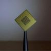
CMOS 2.0,来了
半导体芯闻· 2025-10-20 10:40
Core Viewpoint - The article discusses the advancements in semiconductor technology, particularly the breakthroughs achieved by imec in wafer-to-wafer hybrid bonding and back interconnects, paving the way for CMOS 2.0 technology set to launch in 2024 [1]. Group 1: CMOS 2.0 Technology Core - CMOS 2.0 technology focuses on advanced 3D interconnects and back power delivery networks (BSPDN), enabling high-density connections on both sides of the wafer [2]. - Key milestones presented at the 2025 VLSI symposium include wafer-to-wafer hybrid bonding with a spacing of 250 nanometers (nm) and a back spacing of 120 nm for through-die vias (TDV), addressing performance bottlenecks in AI and mobile applications [2]. Group 2: Wafer-to-Wafer Hybrid Bonding - Wafer-to-wafer hybrid bonding allows for sub-micron spacing, facilitating high bandwidth and low power signal transmission [3]. - The optimized process includes aligning and bonding two processed wafers at room temperature, achieving reliable connections with a spacing of 400 nm using silicon carbon nitride (SiCN) [3]. - imec has reduced bonding spacing to 300 nm with 95% of chip alignment errors under 25 nm, showcasing the feasibility of 250 nm spacing bonding under a hexagonal pad grid architecture [3]. Group 3: Back Interconnect Technology - Back interconnect technology complements front bonding by enabling "front-back" connections through nano-scale silicon vias (nTSV) or direct contact [4]. - This technology allows seamless integration of metal layers on both sides of the wafer, reducing voltage drop and alleviating signal routing congestion in the front-end [4]. - imec demonstrated a back dielectric via (TDV) with a bottom diameter of 20 nm and a spacing of 120 nm, balancing the need for fine spacing connections on both sides of the wafer [4]. Group 4: Advantages of Back Power Delivery Network (BSPDN) - BSPDN enhances CMOS 2.0 performance by relocating power distribution to the back of the wafer, accommodating wider and lower-resistance interconnects [6]. - Research indicates that BSPDN improves power, performance, area, and cost (PPAC) metrics for "always-on" designs and is particularly beneficial for "switch domain" architectures in mobile SoCs [6]. - In 2 nm mobile processor designs, BSPDN reduced voltage drop by 122 millivolts (mV), leading to a 22% area savings while enhancing performance and energy efficiency [6]. Group 5: Technology Implementation and Future Outlook - Supported by pilot lines in nano integrated circuits (NanoIC) and EU funding, these breakthroughs are transitioning CMOS 2.0 from concept to practical application [7]. - The future collaboration with equipment suppliers will be crucial as bonding spacing shrinks below 200 nm to address alignment challenges [7]. - High-density front and back interconnect technologies are expected to usher in a new era of computing innovation, meeting diverse application demands for performance, power, and integration [7].


当算力重构遇上产业变革,这场论坛将定义未来 “芯” 格局
半导体芯闻· 2025-10-20 10:40
Core Insights - The electronic circuit and semiconductor industry is at a critical juncture driven by explosive growth in AI large models and global supply chain restructuring, with a 30-fold increase in computing core numbers over the past decade, while memory bandwidth growth is less than 1/5, leading to storage bottlenecks and material iteration challenges [1] Group 1: Storage Technology Breakthrough - Storage is viewed as the "reservoir" of AI computing power, with breakthroughs in technology directly impacting the efficiency of power release [3] - The forum will focus on three major technological directions: traditional storage upgrades, emerging storage implementations, and RV technology integration [3] Group 2: Material Innovation - Material innovation is the underlying logic for upgrading the semiconductor industry, with the forum addressing core material breakthroughs [4] - Key topics include advancements in AMB copper-clad ceramic substrates, third-generation semiconductors like SiC and GaN, and PCB material breakthroughs to meet high-density demands [5] Group 3: Digital Transformation and Intelligent Manufacturing - The forum will explore the application of AI technology across the entire PCB design, production, and testing process, enhancing defect recognition and production efficiency [5] - Discussions will include AI-based dynamic adjustments of key process parameters and the design logic of AI scheduling systems for flexible manufacturing [5] Group 4: Advanced Packaging and EDA Tools - Advanced packaging and EDA tools are becoming critical for breakthroughs in computing power, with a focus on system-level packaging (SiP) and Chiplet technology integration [7] - The forum will analyze the collaborative mechanisms between academia, research institutions, and enterprises to accelerate the industrialization of innovative results [11] Group 5: Forum Details - The "AI-Driven, Smart Chain Future: 2025 Electronic Circuit and Semiconductor Industry Innovation Forum" will take place on October 28, 2025, at the Shenzhen International Convention and Exhibition Center [10] - The forum will cover topics such as AI + PCB intelligent manufacturing, EDA technology breakthroughs, and the localization of AI computing chips [10]

这颗40岁的芯片,改写历史!
半导体芯闻· 2025-10-20 10:40
Core Insights - The Intel 80386 processor, launched in October 1985, marked a significant turning point in personal computing as the first 32-bit chip in the Intel PC product line and the origin of the IA-32 instruction set [1][5][14] - The 80386 featured 275,000 transistors and operated at a frequency of up to 16 MHz, supporting a maximum address space of 4GB, which laid the foundation for true multitasking and virtual memory [1][4] - The introduction of the 80386 led to the development of various operating systems, including early versions of Windows and Linux, which utilized its advanced features [4][12] Group 1: Historical Context - The 80386 was developed as a response to the competitive landscape, particularly after IBM rejected Intel's earlier designs, leading Compaq to be the first company to launch a computer with the new CPU [2][11] - The Deskpro i386, released by Compaq in September 1986, was priced at $6,499 and became a pivotal product in the PC industry [2][10] - The architecture of the 80386 was influenced by the need for backward compatibility and the desire to create a more powerful and efficient processing unit compared to its predecessors [6][8] Group 2: Technical Advancements - The 80386 introduced a protected mode and paging capabilities, which allowed for better memory management and the ability to run multiple DOS sessions simultaneously [1][4][8] - It expanded the instruction set significantly, adding 54 new instructions and various addressing modes to effectively utilize the 4GB address space [8][10] - The architecture's design enabled the development of a robust ecosystem around the 80386, leading to its widespread adoption in servers and mobile computers [14] Group 3: Market Impact - The 80386's success was crucial for Intel, as it faced significant competition from other manufacturers who were also producing x86-compatible processors [5][12] - By the late 1980s, the 80386 had established itself as a standard in the PC market, leading to the creation of a diverse range of applications and operating systems that leveraged its capabilities [12][14] - The processor's legacy continues today, as modern x86 processors still retain the core architecture established by the 80386, highlighting its lasting influence on computing [14][15]

外媒怒批苹果M5:升级太小
半导体芯闻· 2025-10-20 10:40
Core Insights - Apple's latest product updates, including the M5 chip, show minimal enhancements for consumers, primarily focusing on chip upgrades rather than significant new features [1][4][6] - The company is experiencing talent loss in its AI department, which could pose future challenges as AI becomes a critical factor in consumer purchasing decisions [10][11][12] - Apple is reportedly developing a touch-screen MacBook Pro, indicating a shift in strategy to align with market trends despite previous denials [14][15] Product Updates - The new 14-inch MacBook Pro features the M5 chip, with performance improvements of approximately 15%-20% over the M4, but daily usage differences are negligible [1][4] - The MacBook Pro's updates include slight enhancements in memory bandwidth and SSD speed, with a new 4TB storage option available [4] - The M5 iPad Pro's improvements are limited to the new chip and some internal components, with no significant user experience changes for those already using the M4 version [6] Vision Pro Insights - The Vision Pro headset has seen minimal updates, primarily the M5 chip and a new strap, but remains a niche product with limited appeal [8][9] - The price point of the Vision Pro, starting at $3,499, continues to be a barrier for many consumers, and the lack of substantial improvements may deter existing users from upgrading [8] AI Department Challenges - Apple's AI division is facing significant talent attrition, with key personnel leaving, which could impact the development of AI features like Siri [10][11] - The company is reportedly considering third-party models to address issues within its AI framework, indicating potential instability in its AI strategy [11][12] Touch-Screen MacBook Development - Apple is moving forward with the development of a touch-screen MacBook Pro, a shift from its previous stance against such features [14][15] - The convergence of macOS and iPadOS interfaces suggests that the differences between Mac and iPad may soon be minimal, prompting the need for touch functionality [15]

又一家厂商,跨界AI芯片
半导体芯闻· 2025-10-20 10:40
Core Insights - The article highlights the successful development of a high-performance computing (HPC) system-on-chip (SoC) by 联咏, based on Arm Neoverse CSS N2 architecture, marking a significant milestone for the company in entering the data center, AI cloud, and automotive computing markets [1][3] Group 1: Product Development - The SoC utilizes a "Chiplet" heterogeneous integration architecture, incorporating Neoverse N2 computing cores, DDR5 and HBM3e memory controllers, PCIe 6.0/CXL 2.0 interfaces, and 224G SerDes high-speed transmission modules, enabling a modular design [2] - The SoC is manufactured using TSMC's N4P advanced process and CoWoS advanced packaging, demonstrating 联咏's long-term commitment to high-performance, low-power computing and its capabilities in AI ASIC and Chiplet design services [2] Group 2: Market Position and Growth Potential - Industry insiders note that 联咏's successful transition from consumer ICs to server and ASIC chip development positions it well for entering the AI hardware infrastructure market, with AI server and edge computing demands expected to drive new growth [2][3] - The successful tape-out of the SoC validates 联咏's capabilities in advanced process ASIC integration, laying the groundwork for future developments in cloud AI, automotive autonomous driving, and edge server applications [3] - Analysts are optimistic about the growth potential of 联咏's ASIC business, anticipating an increase in revenue contribution from AI servers and automotive electronics, reinforcing the company's strategic positioning in the high-performance computing market [3]

存储巨头,抢攻9nm!
半导体芯闻· 2025-10-20 10:40
Group 1 - Micron is evaluating two potential roadmap paths for DRAM technology, one following the traditional route to 10.1nm and another ambitious plan to skip directly to 9nm [1] - The current commercial node, 1c, has a line width of approximately 11.2nm, and the ability to reduce the 1d node's line width will determine the feasibility of skipping the 1e node [1] - Competitors Samsung and SK Hynix are also planning to transition directly to 9nm DRAM, prompting Micron to adjust its roadmap to remain competitive [1] Group 2 - 3D DRAM is considered the next breakthrough in storage architecture, but mass production is unlikely before 2033 or 2034 due to delays in achieving the necessary stacking layers [2] - Experts estimate that at least 90 to 100 layers will be needed for 3D DRAM to be commercially viable, while current prototypes are limited to 16 to 24 layers [2] - Chip manufacturers are investing heavily in 4F² and 3D DRAM research and development, but the transition will be gradual due to high technical barriers and manufacturing costs [2] Group 3 - Micron is investing $100 billion in a new wafer fabrication plant in New York, which is the largest private investment in the state's history [3] - The project is expected to create over 50,000 jobs in the next 20 years, with approximately 9,000 direct jobs, and aims to account for about 25% of U.S. semiconductor production [3] - The approval of a new underground power line marks the first phase of construction, aligning with Micron's strategic investment agreement with New York state [3]

本土最强示波器,打破垄断
半导体芯闻· 2025-10-18 01:26
Core Viewpoint - The article highlights the launch of a new 90GHz ultra-high-speed real-time oscilloscope by Wanliyan, a subsidiary of Xinkai, which addresses the critical need for high-bandwidth measurement tools in China's semiconductor and communication industries, previously hindered by Western export controls [1][5][6]. Group 1: Product Features and Innovations - The 90GHz oscilloscope is designed to meet the demands of advanced interface technologies like PCIe 6 and PCIe 7.0, which require high bandwidth for effective signal measurement [3]. - The oscilloscope boasts a sampling rate of 200 billion samples per second, enabling precise capture of picosecond-level transient signals, significantly enhancing measurement accuracy [8]. - It features a storage depth of 4 billion samples, which is double the industry standard, allowing for continuous and uninterrupted recording [8]. - The oscilloscope incorporates an innovative "smart parameter optimization" function, which can explore thousands of configurations in just 10 minutes, increasing testing efficiency by over 100 times [8]. - It is the first oscilloscope to feature a full-screen design with an 18.5-inch display, supporting multi-touch interaction for a more intuitive user experience [8]. Group 2: Strategic Focus and Market Position - Wanliyan was established to address the "bottleneck" issues in high-end measurement instruments due to export restrictions from Western countries, which have limited access to advanced electronic measurement tools in China [5][6]. - The company focuses on seven key technological areas, including critical components, advanced materials, manufacturing processes, system integration, software, intelligent algorithms, and protocol capabilities, to ensure the successful development of high-end measurement instruments [10]. - Wanliyan aims to provide innovative testing solutions across three main fields: basic measurement instruments, RF microwave measurement instruments, and network testing instruments, with a total of eight product series [10][11]. - The company has gained recognition from various clients, including universities and research institutions, and is capable of providing stable and bulk services [11]. Group 3: Future Outlook and Vision - The company emphasizes the importance of rapid iteration and responsiveness to customer needs as a competitive advantage, aiming to maintain close communication with clients to enhance product applications and innovations [12]. - Wanliyan is committed to continuous investment in technology innovation across materials, processes, chips, systems, algorithms, protocols, and software, collaborating with industry partners to advance technology and industry progress [12]. - The CEO expresses confidence in transitioning from a follower to a leader in the industry, aiming to serve the entire industry chain effectively [12].

AMD Helios 机架,首次曝光
半导体芯闻· 2025-10-18 01:26
Core Insights - AMD has announced a significant agreement with Oracle for 50,000 GPUs and showcased its upcoming super AI rack planned for the second half of 2026 [1][33] - The AMD Helios rack has notable design differences compared to Meta's version, particularly in power distribution and network layout [33] Group 1: AMD Helios Rack Features - The AMD Helios rack features a management switch and power supply at the top, with a power shelf containing compute nodes below [3][5] - The design includes a robust handle on the switch tray, indicating a focus on durability [9] - The rack utilizes EDSFF E1.S SSDs and has transitioned from 2.5-inch U.2 connectors in PCIe Gen6 [10] Group 2: Comparison with Meta's Rack - Meta's rack design differs significantly, with Ethernet switches placed at the top instead of power supplies, indicating a major architectural change [15][16] - The internal arrangement of power and network components in Meta's rack allows for a more efficient power delivery system [29] - Both racks share similarities in width and the sandwich layout of compute and switch trays, but the internal configurations are distinct [33] Group 3: Performance Metrics - AMD's Helios AI rack is equipped with the MI400 series, boasting 72 GPU domains, 260 TB/s scale-up bandwidth, and 2.9 EF FP4 and 1.4 EF FP8 FLOPS [35] - The HBM4 memory capacity is 31 TB with a memory bandwidth of 1.4 PB/s, showcasing AMD's competitive edge in high-performance computing [35] - The Helios AI rack has attracted significant investment interest from major AI companies [36]

突发,安世中国员工被断发工资,荷兰有意与中国谈判
半导体芯闻· 2025-10-18 01:26
Core Viewpoint - The Dutch Minister of Economic Affairs, Karremans, is seeking to negotiate with China to resolve the export ban on Nexperia chips, which is critical for global automotive manufacturers [1][2]. Group 1: Export Ban and Its Implications - The export ban on Nexperia chips, effective this week, follows the Dutch government's takeover of the company, leading to the dismissal of its Chinese CEO, Zhang Xuezheng [1]. - Nexperia, acquired by China's Wingtech Technology in 2019, produces over 50 billion chips annually, and the ban could lead to significant shortages in automotive electronics within weeks [1][2]. - The American Automotive Innovation Alliance has warned that supply issues may arise soon, affecting major manufacturers like BMW and Volkswagen [2]. Group 2: Importance of Chips in Automotive Industry - The European Automobile Manufacturers Association (ACEA) has expressed concerns that without chips, European automotive suppliers cannot produce necessary components, potentially halting production [3]. - Karremans emphasized the importance of ensuring Nexperia can navigate this crisis, aligning with the interests of the US, Netherlands, Europe, and China [3]. Group 3: Company Developments - Nexperia's situation has led to significant operational disruptions, with reports indicating that Nexperia's Chinese subsidiary, Anshi Semiconductor, has halted salary payments and lost system access [5].
全球智驾芯片TOP 5:华为、地平线上榜
半导体芯闻· 2025-10-18 01:26
Core Insights - The global automotive SoC market is entering a rapid growth phase, with major suppliers like Mobileye, NVIDIA, Qualcomm, Horizon, and Huawei expected to dominate the market by 2035, increasing their combined market share from 69% in 2025 to over 78% [1] - The demand for high-performance SoCs is driven by the need for AI perception, sensor fusion, and redundancy in higher levels of autonomous driving [1][2] - Chinese SoC manufacturers Horizon and Huawei are projected to capture over 50% of the domestic market by 2035 through the rapid expansion of cost-effective L2+ and above SoCs [1] Group 1 - Mobileye's cost-competitive products are anticipated to gain wider adoption in emerging markets such as India, Southeast Asia, Latin America, and the Middle East, helping it maintain its leadership in the L2 ADAS sector [2] - The shift towards centralized electrical architectures by automotive manufacturers is expected to sustain the demand for high-performance SoCs, particularly for L3 and L4 autonomous driving levels [2] - NVIDIA, Qualcomm, and Huawei are expected to see significant market share growth, with a compound annual growth rate exceeding 15% during the forecast period due to their superior and flexible SoC products [2] Group 2 - The automotive market is expected to become more fragmented by 2035, with high computational demand for vehicles projected to grow 3-4 times compared to current levels [4] - SoC suppliers that can balance AI performance, energy efficiency, and cost competitiveness are likely to succeed in the evolving market [4] - OEMs are expected to adopt multi-source strategies to optimize costs for L2 and L2+ autonomous driving chips while managing the costs of high-performance SoCs required for advanced autonomous driving products [4]
